
COMPLETE STC-NT SIC-BASED DEVICE PRODUCTION CHAIN: FROM THEORY TO PRACTICE
DESIGN & SIMULATION
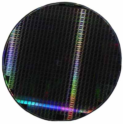
MATERIALS & SUBSTRATES
• Growth of SiC/Si substrates by the method of atoms
substitution
• Growth of GaN, AlN, AlGaN, ZnO, CdSe, CdTe thin
films, heterostructures or bulk crystals on SiC/Si
• Growth of semipolar films
PROCESS/DIES
SYSTEMS/MODULES
• Optoelectronic devices, blue lasers, power LED’s.
• Photosensors, UV-detectors, flash memory
• Microwave devices, mobile phones, satellite TV, radars,
• Field-effect transistors, microprocessors, microwave ovens
• High-voltage devices and power sources.
• High-power devices for trains and power lines
• Membranes for microphones, pyro-matrices for night vision devices
Challenges
Miniaturization of devices
Price reduction of devices,
which are based on SiC and
III-nitrides
Reduction of electronic device
power consumption
Operation of the unit in
aggressive environments:
under irradiation, in space, at
high temperature, humidity,
acidity
• Processing of chips
• E-beam or optical lithography
• Application of contacts and additional masks
• Advanced LED process
• Integrated circuit formation process
• Theoretical investigation of crystal growth process
• Modeling of flows and chemical reactions during crystal synthesis in reactor
• Simulation of crystal growth process
• Simulation of semiconductor compound properties using quantum chemistry
• Calculation of parameters for growth of structures with desired properties
Preparation of Si surface using layers of mono- and
dihydrosilicon
Preliminary heatinf in reactor at the pressure in vacuum in range 10
-2
-10
-3
Pa and
temperature T=800
o
C
CO gas pumping to the reactor. Heating up to working temperature up to 950-
1350
o
С. Synthesis due to reaction:
2Si(solid)+CO(gas) = SiC(solid)+SiO(gas)
Epi-ready SiC/Si
HVPE
MOCVD
CVD
AlN and GaN/AlN on SiC/Si
SiC (3-25 um) on SiC/Si
Raw Si
Patented technology
Solid state chemical
reacton of Si and CO
Modificated
method of
sublimation
Heteroepitaxy of
SiC on Si
Vapor Liquid
Solid
(VLS)
High-temperature
chemical deposition
(HT-CVD)
Liquid phase
epitaxy (LPE)
Max.diameter(todate)
200
125 200 50 50 50
Thickness,um
30
60 0,5 1-2 20 5
Polytype
3C,4H,6H
4Н,6Н 3C 3C 4Н,6Н 4Н
Growthtemperature,°C
1000–1350
2200-2500 1350 1100 2200 1460-1800
Manufacturers
STCNT
Cree,SiCrystal,II-
VI,etc.
Hoya,
Toshiba,Ceramics
CRHEA Norstel SumitomoToyota
Developmentstage
R&D
Industrial
production
R&D R&D R&D R&D
Price using traditional technology:
>$1000 per 4 inch wafer
~2600 $ per substrate with
3600 chips
~ 1500 $ (10 um in
thickness)
Production of SiC/Si
substrates
Production of SiC with EPI
Processing of chips
Cost of processing, packaging and
testing of a SiC wafer is ~800$
Production cost using STC NT
technology is 10 times lower
Packaged device/component
Power module
$ 26-36 depending on
application
$ 1,4-24 depending on application
The products developed by STC NT have significant advantages, which will allow:
• Extend the use of existing products (including LEDs)
• Discover new applications
• Compete successfully in the market
Wafer suppliers
Device manufacturers
Manufacturers of devices and modules
STC NT, CREE, Dow Corning (USA), SiCrystal (Germany),etc.
CREE, MicroSemi, Fairchild, GeneSiC, SemiSouth(USA), STM
(Italy), etc.
Powerex, MicroSemi (USA), STM (Italy), ABB
(Sweden),etc.
Role of “STC NT” in the market
Quality of epitaxy significantly
affects the price
The technology
Competitive Advantages of SiC/Si Growth Technology
Nanoscale silicon carbide – new material for micro- and optoelectronics
SiC applications
Electronics for hybrid and
electrocars
Wind generators
Acoustic sensors on segnetoelectrics
Uninterruptible Power Supply
Solar energy converters
Schottky diodes in PFC devices
High Brightness LEDs (GaN/SiС)
Smart Grid Power Rail
transport
2018 > 2022
Si SOI
(silicon on
insulator)
SiC GaN (on
silicon)
Maxusagetemperature
125 225 400
350forGaN,limited
bySi
Powerrange >100kW <100kW >100kW >5kW
Max.voltage 6.5kV 600V 10kV 1.2kV
4”waferprice,$ 20 70 950$* <250
6”waferprice,$ 35 170 na <400
Numberofcompanies,developing
devicesonthematerial
100+ ~40 ~25 ~15
Why SiC, not other materials?
Market of SiC wafers and epitaxial structures
The main market growth drivers in 2019:
• Hybrid and electro-propulsion systems – market volume ~$270 million
• Invertors for solar cells - $91 million.
• Microwave devices - $48 million.
Source: Yole development
ABOUT US